


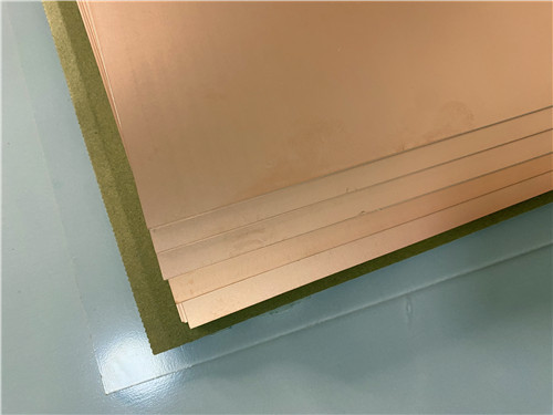

RO3006 Hochfrequenz-PCB-Laminat: Dk 6.15, geringer Verlust und CTE mit Kupfer für kompakte HF-Designs abgestimmt
ContPerson : Sally Mao
Telefonnummer : 86-755-27374847
- Was ist? : +8618277967574
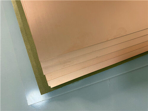
| Markenname: | Rogers | Modellnummer: | TMM10i |
|---|
Produkt-Beschreibung
Es ist ein keramikgefülltes Duroplast-Mikrowellenlaminat, hergestellt von Rogers Corporation. Es ist Teil der TMM®-Serie. Die Dielektrizitätskonstante (Dk) beträgt 9,80 ±0,245 bei 10 GHz. Der Verlustfaktor (Df) beträgt 0,0020 bei 10 GHz. Das Material hat eine isotrope Dielektrizitätskonstante. Der CTE beträgt 19 ppm/°C in allen Richtungen (X, Y und Z). Dies entspricht dem CTE von Kupfer. Die Zersetzungstemperatur (Td) beträgt 425°C. Die Wärmeleitfähigkeit beträgt 0,76 W/(m·K). Das Material ist ein Duroplast-Harz. Es erweicht bei Erwärmung nicht. Drahtbonden kann ohne Bedenken hinsichtlich Pad-Lifting oder Substratverformung durchgeführt werden. Vor der chemischen Vernickelung ist keine Natriumnaphtanat-Behandlung erforderlich.
Welche Leiterplatte kann damit hergestellt werden?
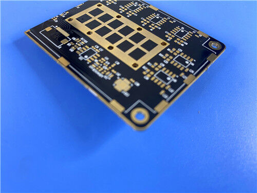
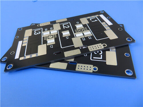
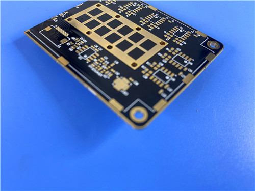
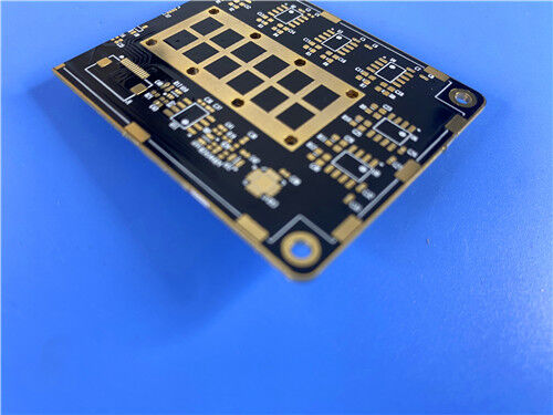
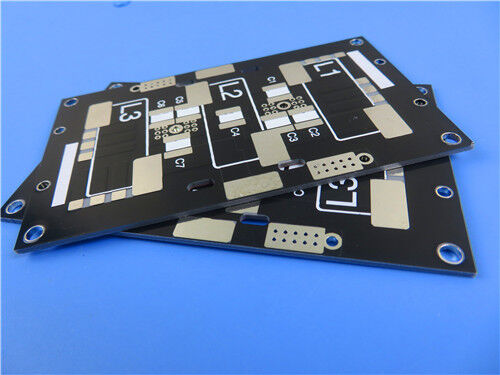
Eine komplette 2-lagige RF-Leiterplattenlösung kann bereitgestellt werden. Die Leiterplatte basiert auf TMM10i-Material. Die Fertigdicke beträgt 0,8 mm. Das Kupfergewicht beträgt 1 oz pro Lage. ENIG (chemisch Nickel/Immersion Gold) wird als Oberflächenveredelung angewendet. Schwarze Lötmaske wird auf beiden Seiten aufgetragen. Weiße Siebdruckfarbe wird auf beiden Seiten aufgedruckt. Randplattierung wird angewendet. Die minimale Leiterbahnbreite und der minimale Leiterbahnabstand betragen 6 bzw. 9 mils. Die minimale Lochgröße beträgt 0,4 mm. Die Dicke der Via-Plattierung beträgt 20 µm. Der Qualitätsstandard ist IPC Klasse 2. Diese Leiterplatte ist ideal für RF/Mikrowellenschaltungen, Leistungsverstärker, Filter, Satellitenkommunikationssysteme, GPS-Antennen und Chip-Tester.
1. Materialübersicht
TMM10i ist ein Duroplast-Mikrowellenmaterial. Es wird von Rogers Corporation hergestellt. Es ist Teil der TMM®-Serie. Es ist ein keramikgefüllter Kohlenwasserstoff-Duroplast-Polymerverbundwerkstoff. Es ist für hohe Zuverlässigkeit von durchkontaktierten Bohrungen ausgelegt. Es ist für Stripline- und Microstrip-Anwendungen geeignet.
Die TMM-Serie kombiniert viele der wünschenswerten Eigenschaften von Keramiksubstraten mit der einfachen Verarbeitung von weichen Substraten. Es erfordert keine speziellen Produktionstechniken. Es erfordert keine Natriumnaphtanat-Behandlung vor der chemischen Vernickelung. Dies reduziert die Komplexität und die Kosten der Fertigung.
Hauptmerkmale von TMM10i:
Isotrope Dielektrizitätskonstante — Die Dk ist in allen Richtungen gleich. Dies vereinfacht das Design und gewährleistet eine konsistente Leistung.
Hohe Dielektrizitätskonstante — Die Dk beträgt 9,80 ±0,245. Dies ermöglicht kleinere Schaltungsgrößen.
Niedriger Verlustfaktor — Der Df beträgt 0,0020 bei 10 GHz. Signalverluste werden minimiert.
Kupfer-angepasster CTE — Der CTE beträgt 19 ppm/°C in allen Richtungen. Dies entspricht dem CTE von Kupfer. Hervorragende Dimensionsstabilität wird erreicht. Hohe Zuverlässigkeit von durchkontaktierten Bohrungen wird gewährleistet.
Duroplast-Harz — Das Material erweicht bei Erwärmung nicht. Drahtbonden kann ohne Bedenken hinsichtlich Pad-Lifting oder Substratverformung durchgeführt werden.
Wärmeleitfähigkeit — Die Wärmeleitfähigkeit beträgt 0,76 W/(m·K). Dies ist etwa doppelt so hoch wie bei herkömmlichen PTFE/Keramik-Laminaten. Die Wärmeableitung wird erleichtert.
Chemische Beständigkeit — Das Material ist beständig gegen Ätzmittel und Lösungsmittel. Alle gängigen Leiterplattenprozesse können verwendet werden.
Kriech- und Kaltflussbeständigkeit — Die mechanischen Eigenschaften widerstehen Kriechen und Kaltfluss. Die Dimensionsstabilität wird über die Zeit aufrechterhalten.
2. TMM10i Technisches Datenblatt
| Eigenschaft | Typischer Wert | Richtung | Einheiten | Bedingung | Prüfmethode |
| Dielektrizitätskonstante (Prozess) | 9,80 ±0,245 | Z | — | 10 GHz | IPC-TM-650 2.5.5.5 |
| Dielektrizitätskonstante (Design) | 9,9 | — | — | 8–40 GHz | Differenzielle Phasenlänge |
| Verlustfaktor | 0,002 | Z | — | 10 GHz | IPC-TM-650 2.5.5.5 |
| TCDk | -43 | — | ppm/°K | -55 bis +125°C | IPC-TM-650 2.5.5.5 |
| Isolationswiderstand | >2000 | — | GΩ | C/96/60/95 | ASTM D257 |
| Volumenwiderstand | 2×10⁸ | — | MΩ·cm | — | ASTM D257 |
| Oberflächenwiderstand | 4×10⁷ | — | MΩ | — | ASTM D257 |
| Durchschlagsfestigkeit | 267 | Z | V/mil | — | IPC-TM-650 2.5.6.2 |
| Zersetzungstemperatur (Td) | 425 | — | °C | — | ASTM D3850 |
| CTE X-Achse | 19 | X | ppm/K | 0 bis 140°C | ASTM E 831 / IPC-TM-650 2.4.41 |
| CTE Y-Achse | 19 | Y | ppm/K | 0 bis 140°C | ASTM E 831 / IPC-TM-650 2.4.41 |
| CTE Z-Achse | 20 | Z | ppm/K | 0 bis 140°C | ASTM E 831 / IPC-TM-650 2.4.41 |
| Wärmeleitfähigkeit | 0,76 | Z | W/(m·K) | 80°C | ASTM C518 |
| Kupfer-Abziehfestigkeit | 5,0 (0,9) | X,Y | lb/in (N/mm) | nach Lötbad | IPC-TM-650 2.4.8 |
| Biege-Elastizitätsmodul | 1,8 | X,Y | Mpsi | A | ASTM D790 |
| Feuchtigkeitsaufnahme (1,27 mm) | 0,16 | — | % | D/24/23 | ASTM D570 |
| Feuchtigkeitsaufnahme (3,18 mm) | 0,13 | — | % | D/24/23 | ASTM D570 |
| Spezifisches Gewicht | 2,77 | — | — | A | ASTM D792 |
| Spezifische Wärmekapazität | 0,72 | — | J/g/K | A | Berechnet |
| Bleifreie Prozesskompatibilität | JA | — | — | — | — |
3. Hauptvorteile von TMM10i
| Merkmal | Nutzen |
| Dk ist 9,80 ±0,245 | Hohe Dk ermöglicht kleinere Schaltungsgrößen; isotrope Dk vereinfacht das Design |
| Df ist 0,0020 bei 10 GHz | Geringe Verluste minimieren die Signalabschwächung in Mikrowellenschaltungen |
| CTE ist 19 ppm/°C (X/Y/Z) | CTE passt zu Kupfer; hervorragende Dimensionsstabilität; hohe Zuverlässigkeit von PTHs |
| TCDk ist -43 ppm/°K | Stabile Dk über die Temperatur gewährleistet konsistente Leistung |
| Td ist 425°C | Außergewöhnliche Beständigkeit gegen thermische Zersetzung wird geboten |
| Wärmeleitfähigkeit ist 0,76 W/(m·K) | Wärmeableitung ist im Vergleich zu Standard-PTFE verbessert |
| Duroplast-Harz wird verwendet | Kein Erweichen bei Erwärmung; zuverlässiges Drahtbonden; kein Pad-Lifting |
| Keine Natriumnaphtanat-Behandlung erforderlich | Standardverarbeitung wird verwendet; Fertigung wird vereinfacht |
| Beständig gegen Kriechen und Kaltfluss | Langzeit-Dimensionsstabilität wird aufrechterhalten |
| Chemische Beständigkeit wird geboten | Beschädigung während der Fertigung wird reduziert |
4. Anwendungsbereiche
- RF- und Mikrowellenschaltungen
- Leistungsverstärker und -kombinierer
- Filter und Koppler
- Satellitenkommunikationssysteme
- Global Positioning System Antennen
- Patch-Antennen
- Dielektrische Polarisatoren und Linsen
- Chip-Tester
5. Kundenspezifische 2-lagige RF-Leiterplatte – Vollständige Spezifikation
Eine komplette 2-lagige RF-Leiterplattenlösung auf Basis von TMM10i kann bereitgestellt werden. Die Spezifikationen sind unten aufgeführt.
Leiterplattenspezifikationen
| Spezifikation | Detail |
| Leiterplattentyp | 2-lagige RF-Leiterplatte |
| Basismaterial | Rogers TMM10i (0,762 mm / 30 mil Kern) |
| Fertige Leiterplattendicke | 0,8 mm |
| Fertiges Kupfergewicht | 1 oz (35 µm) pro Lage |
| Leiterplattengröße | 104,8 × 99,01 mm (1 Stück) |
| Maßtoleranz | ±0,15 mm |
| Minimale Leiterbahnbreite / -abstand | 6 / 9 mils |
| Minimale Lochgröße | 0,4 mm |
| Via-Plattierungsdicke | 20 µm |
| Oberflächenveredelung | ENIG (chemisch Nickel/Immersion Gold) |
| Obere Lötmaske | Schwarz |
| Untere Lötmaske | Schwarz |
| Obere Siebdruckfarbe | Weiß |
| Untere Siebdruckfarbe | Weiß |
| Randplattierung | Ja |
| IPC-Klassifizierung | Klasse 2 |
| Artwork-Format | Gerber RS-274-X |
| Prüfung | 100% elektrische Prüfung (vor Versand) |
| Verfügbarkeit | Weltweit |
6. Hauptvorteile dieses Leiterplattendesigns
| Merkmal | Nutzen |
| 2-lagiges RF-Design wird verwendet | Einfache und kostengünstige Implementierung von RF-Schaltungen wird erreicht |
| TMM10i-Kern (0,762 mm) wird verwendet | Hohe Dk (9,8) ermöglicht kleinere Schaltungsgrößen; geringe Verluste (0,0020) gewährleisten Signalintegrität |
| 6/9 mil Leiterbahnbreite und -abstand werden verwendet | Feinlinige, hochdichte RF-Schaltungen können hergestellt werden |
| Schwarze Lötmaske wird auf beiden Seiten aufgetragen | Professionelles Aussehen; Schutz der Schaltung auf beiden Seiten |
| ENIG-Veredelung wird angewendet | Hervorragende Lötbarkeit; Oxidationsbeständigkeit; ebene Oberfläche |
| Randplattierung wird angewendet | Abschirmung und Erdung werden verbessert |
| 20 µm Via-Plattierung wird verwendet | Zuverlässige durchkontaktierte Verbindungen werden gewährleistet |
| IPC Klasse 2 Qualität wird erfüllt | Kommerzielle und industrielle Qualitätsstandards werden erfüllt |
| 100% elektrische Prüfung wird durchgeführt | Funktionale Integrität wird vor dem Versand garantiert |
7. Warum Randplattierung verwendet wird
Randplattierung wird auf dieser Leiterplatte angewendet. Die Vorteile sind unten aufgeführt.
| Vorteil | Nutzen |
| Abschirmung wird verbessert | RF-Signale werden eingeschlossen; EMI wird reduziert |
| Erdung wird ermöglicht | Direkte Chassis-Erdung ist möglich |
| Mechanische Festigkeit wird verbessert | Leiterplattenkanten werden geschützt |
| Lötbarkeit wird geboten | Randverbindungen können gelötet werden |
Vergleichstabelle – TMM10i vs. TMM10 vs. TMM6
| Parameter | TMM10i | TMM10 | TMM6 |
| Dk bei 10 GHz | 9,80 ±0,245 | 9,20 ±0,23 | 6,00 ±0,15 |
| Df bei 10 GHz | 0,002 | 0,002 | 0,002 |
| CTE X/Y (ppm/°C) | 19/19 | 19/19 | 19/19 |
| CTE Z (ppm/°C) | 20 | 20 | 20 |
| Td (°C) | 425 | 425 | 425 |
| Wärmeleitfähigkeit (W/m·K) | 0,76 | 0,76 | 0,76 |
| Isotrope Dk | Ja | Ja | Ja |
| Primäre Verwendung | Hohe Dk RF, Aluminiumoxid-Ersatz | Hohe Dk RF | Mittlere Dk RF |
F1: Was ist die Dielektrizitätskonstante von TMM10i?
Die Prozess-Dk beträgt 9,80 ±0,245 bei 10 GHz. Die Design-Dk beträgt 9,9 von 8 GHz bis 40 GHz. Die Dk ist isotrop. Das bedeutet, sie ist in allen Richtungen (X, Y und Z) gleich. Dies vereinfacht das Design und gewährleistet eine konsistente Leistung.
F2: Was ist der Verlustfaktor von TMM10i?
Der Verlustfaktor (Df) beträgt 0,0020 bei 10 GHz. Dieser geringe Verlust minimiert die Signalabschwächung in Mikrowellenschaltungen.
F3: Warum ist der CTE von TMM10i wichtig?
Der CTE beträgt 19 ppm/°C in allen Richtungen (X, Y und Z). Dies entspricht dem CTE von Kupfer. Hervorragende Dimensionsstabilität wird geboten. Hohe Zuverlässigkeit von durchkontaktierten Bohrungen wird gewährleistet. Dies ist wichtig für Leiterplatten, die Temperaturschwankungen ausgesetzt sind.
F4: Warum ist TMM10i ein Duroplast-Material und warum ist das wichtig?
TMM10i basiert auf einem Duroplast-Harz. Es erweicht bei Erwärmung nicht. Drahtbonden von Bauteilanschlüssen an Schaltungspfade kann ohne Bedenken hinsichtlich Pad-Lifting oder Substratverformung durchgeführt werden. Dies ist ein erheblicher Vorteil gegenüber PTFE-basierten Materialien.
Bereit zum Start?
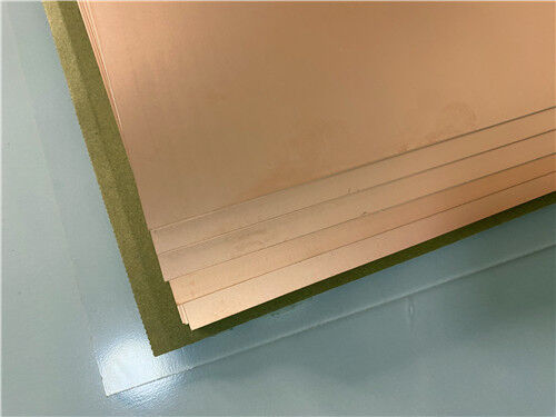
TMM10i Rohlaminat kann bereitgestellt werden. Vollständig gefertigte 2-lagige RF-Leiterplatten mit ENIG-Veredelung und Randplattierung können hergestellt werden.
Kontaktieren Sie uns noch heute für:
Materialmuster und -tests
Unterstützung beim RF-Schaltungsdesign
Impedanzberechnung und Designunterstützung
Leiterplattenangebot und DFM-Prüfung
Technischer Support für Ihre spezifische Anwendung
Tragen Sie Ihre Mitteilung ein

Rogers PWB RO4350B, 4003C; Rogers 5880, 5870, 6002, 6010, 6006, 6035; RO3003, RO3035, RO3006, RO3010, RO3210
Takonisches PWB TLX-8, TLX-6, TLX-9, TLX-0, TLX-7, TLY-3, TLY-5, RF-35TC, RF-60TC, RF-35A2, RF-60A, AD450, AD600, TMM4
| Shenzhen Bicheng Electronics Technology Co., Ltd |
| 6-11C Shidai Jingyuan Fuyong Stadt, Baoan-Bezirk, Shenzhen-Stadt, Provinz Guangdong, China |
| 86-755-27374946 |
| sales30@bichengpcb.com |